* УТОЧНЯЙТЕ ВОЗМОЖНОСТЬ, ЦЕНУ И СРОК ПОСТАВКИ, В СВЯЗИ С ОГРАНИЧЕНИЕМ ЭКСПОРТА ТОВАРОВ ИЗ СТРАН ЕС И ВЕЛИКОБРИТАНИИ
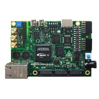
MAX 10 FPGA Development Kit, Altera
The Altera MAX 10 FPGA development kit is a full featured design platform built around a 50 K logic elements (LEs). It is optimised for system level integration with on-die ADC, dual-configuration flash, and DDR3 memory interface support. It has a range of connectivity options including an on-board USB-Blaster II, HDMI output, and dual Ethernet for industrial Ethernet applications. The MAX 10 FPGA Development Kit provides a system-level prototyping solution for industrial, automotive and consumer applications.
With the Altera MAX 10 FPGA Development Kit, you can:
- Develop designs for the 10M50D, F484 package FPGA
- Measure the performance of the MAX 10 FPGA ADC block conversion
- Interface MAX 10 FPGAs to DDR3 memory at 300 MHz performance
- Run embedded Linux using the Nios II processor
- Interface to daughter cards and peripherals using HSMC and Digilent Pmod Compatible connectors
- Measure FPGA power using the power monitor graphical user interface (GUI)
- Reuse the PCB board and schematic as a model for your design
Programming and Configuration
- Embedded USB-Blaster II (JTAG)
- Optional JTAG direct via 10-pin header
Memory Devices
- 64-Mx16 1 GB DDR3 SDRAM with soft memory controller
- 128-Mx8 1 GB DDR3 SDRAM with soft memory controller
- 512 MB Quad serial peripheral interface (quad SPI) flash
Communication Ports
- 2 x Gigabit Ethernet RJ-45 ports
- mini-USB2.0 UART
- HDMI video output
- Universal high-speed mezzanine card (HSMC) connector
- 2 x 12-pin Digilent Pmod compatible connectors
Analogue
- 2 x MAX 10 FPGA ADC SMA inputs
- 2 x 10 ADC header
- Potentiometer input to ADC
- External 16-bit DAC with SMA output
Clocking
- 25 MHz single-ended, external oscillator clock source
- Silicon labs clock generator
Supplied with
- Mini USB cable for on-board USB-Blaster II
- 2A Power Supply and cable
- Free Quartus II Web Edition design software
Featured Devices
An FPGA is a semiconductor device consisting of a matrix of Configurable Logic Blocks (CLBs) connected through programmable interconnects. The user determines these interconnections by programming SRAM. A CLB can be simple (AND, OR gates, etc) or complex (a block of RAM). The FPGA allows changes to be made to a design even after the device is soldered into a PCB.
Техническая спецификация MAX 10 FPGA Development Kit User Guide
| Самовывоз со склада поставщика в Екатеринбурге | Забираете сами или вызываете курьера |
| ТК Деловые Линии | от 500 руб |
| Курьером EMS Почта России | от 500 руб |
| Другой транспортной компанией | По согласованию |

